
 Kontakt
 Jak kupować
Dostawa
Doradca ds. zakupów
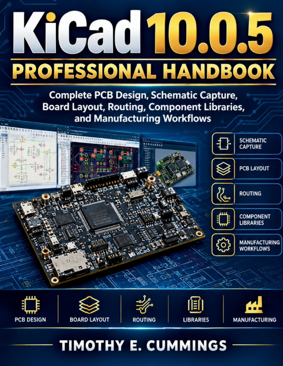
KiCad 10.0.5 Professional Handbook
Complete PCB Design, Schematic Capture, Board Layout, Routing, Component Libraries, and Manufacturing Workflows
 Angielski
 72 b
72 b
 Zapowiedź
 Nowość
Nawet do 30 dni na zwrot

Are you looking for a practical way to design, develop, verify, document, and prepare professional printed circuit boards with KiCad 10.0.5?
Do you want to move beyond basic schematic drawing and learn how the complete PCB development process fits together-from project organization and component libraries to advanced board layout, verification, manufacturing preparation, and production release?
KiCad 10.0.5 Professional Handbook is designed for readers who want a structured, practical reference for developing serious electronic design projects with KiCad 10.0.5. Instead of concentrating only on individual tools, this book follows the complete engineering workflow and explains how the different stages of PCB development connect.
How should a project be organized before detailed design begins? How can schematic architecture support a clean PCB layout? How do you choose and manage reliable symbols, footprints, and 3D models? What should you check before sending a board to manufacturing? How can you identify problems before they become expensive production issues?
This handbook addresses these questions through a professional approach to PCB development.
You will learn how to work with project structure, schematic architecture, PCB layout, design rules, routing, signal integrity considerations, circuit verification, reusable design structures, library engineering, advanced PCB editor capabilities, automation, scripting, external design integration, three-dimensional inspection, mechanical considerations, manufacturing outputs, assembly information, DFM practices, troubleshooting, optimization, and production release workflows.
The book also explains how to approach complex projects systematically. Rather than treating PCB design as a sequence of disconnected commands, it presents the reasoning behind important engineering decisions and shows how electrical, physical, mechanical, manufacturing, and documentation requirements influence one another.
You will explore topics such as:
Building organized PCB projects and maintaining a reliable design structure
Developing clear and maintainable schematics
Creating effective component and connectivity architectures
Assigning and managing symbols, footprints, and three-dimensional models
Planning professional PCB placement and routing
Working with design rules, clearances, copper structures, and routing constraints
Applying practical approaches to signal integrity and critical connections
Using circuit simulation and electrical verification where appropriate
Developing reusable design blocks and repeated circuit structures
Working with multichannel and variant-based designs
Using advanced PCB editor capabilities for complex board development
Applying automation and command-line workflows to repetitive engineering tasks
Understanding scripting and modern automation approaches
Integrating PCB information with external design and mechanical workflows
Reviewing boards through three-dimensional visualization
Checking component height, connectors, mounting features, and enclosure relationships
Preparing professional fabrication and assembly documentation
Generating manufacturing data and reviewing production outputs
Applying design-for-manufacturability principles
Preparing placement information and component documentation
Troubleshooting schematic, PCB, library, routing, zone, and manufacturing problems
Optimizing designs without compromising electrical or mechanical requirements
Establishing repeatable production-release procedures


Informacje o książce
Angielski

Podaruj tę książkę jeszcze dziś
To łatwe
1 Dodaj książkę do koszyka i wybierz „dostarczyć jako prezent” 2 W odpowiedzi wyślemy Ci bon 3 Książka dotrze na adres obdarowanegoCześć! Jestem Libroamiko, Twój doradca książkowy.
Jak mogę Ci pomóc?